MicroZed Chronicles: Imaging with AMD Artix™ 7 FPGA & AMD Artix™ UltraScale+™ FPGA
- Adam Taylor

- Jul 16, 2025
- 4 min read
If you follow my Hackster projects, you’ll know that one area that significantly interests me is image processing applications.
Two of these projects recently got me thinking. The first was an older project where I created an imaging system on the AMD Artix™ 7 FPGA AC701 evaluation kit. I later extended this project for Mouser by implementing a new image processing filter designed to enhance edge clarity. I implemented this filter using MathWorks Simulink.
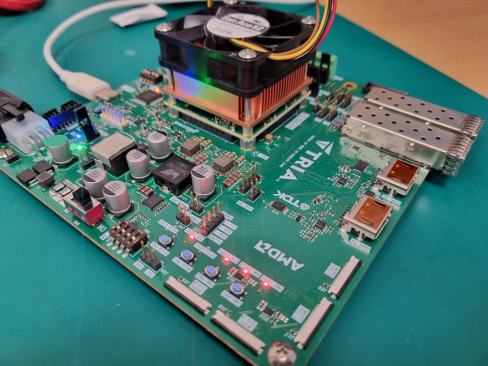
More recently, I created another image processing project using the AUBoard-15P from Tria (formerly Avnet). This board features an AMD Artix UltraScale+™ FPGA.
I thought it would be a good idea to compare the designs implemented on both the Artix 7 FPGA and Artix UltraScale+ FPGA platforms.


Architectural Differences
Naturally, there are some clear differences between the Artix 7 FPGA and Artix UltraScale+ FPGA architectures. These families are fabricated on different process nodes: 28 nm for Artix 7 FPGA and 16 nm for Artix UltraScale+ FPGA. As a result, the Artix UltraScale+ devices offer improved speed and lower power consumption.
The Artix UltraScale+ FPGA also introduces enhancements to the clocking architecture, enabling higher performance and more efficient resource utilization. Notably, the AMD UltraScale™ architecture introduces the BUFGCE and BUFGCE_DIV, the latter of which supports integer clock division without needing MMCMs, PLLs, or additional logic.
Another key improvement is the inclusion of the next generation DSP48 block (DSP48E2) in Artix UltraScale+ FPGAs. These blocks support wider input vectors and new operational modes, which can reduce the number of DSP elements required for image processing algorithms.
Similarly, UltraScale+ device BRAMs have evolved. Larger BRAMs, often used as line buffers, can now be cascaded more efficiently without additional logic, improving both performance and resource utilization.
Interface Considerations
There are also more subtle but important differences. In the original imaging application, MIPI was used to capture images into the processing pipeline. Artix 7 FPGAs require external resistor networks or an external DPHY chip to create a compliant interface (see XAPP894). The compliant solution used on the Artix 7 FPGA AC701 evaluation kit board supports speeds of up to 800 Mbps.
Artix UltraScale+ FPGAs, on the other hand, feature a built-in DPHY within the AMD UltraScale™ architecture SelectIO. This not only saves I/O pins, since it eliminates the need for separate high-speed and low-speed pairs, but also enables image sensors to operate at up to 2 Gbps. The Artix UltraScale+ FPGA also supports other popular image sensor interfaces such as SLVS-EC and Sub-LVDS.
Transceivers and Video Standards
Both Artix 7 FPGAs and Artix UltraScale+ FPGAs provide high-speed serial transceivers, although the supported line rates differ. Artix 7 FPGAs can handle video standards such as SD and HD-SDI, while Artix UltraScale+ FPGAs are capable of supporting higher-bandwidth formats, including 4K imaging, as demonstrated in the recent AUBoard-15P project.
Device Selection: Which One to Select?
As with most engineering applications, selecting between Artix 7 FPGA and Artix UltraScale+™ FPGA depends on specific system requirements. These may include logic resources, functionality, power consumption, and size constraints.
Artix 7 FPGAs are well suited for imaging applications where MIPI line rates are below 800 Mbps and transceivers operate at up to 6 Gbps. When it comes pricing, an Artix 7 device with similar logic resources to the a Artic UltraScale+ FPGA is often more cost effective.
In contrast, Artix UltraScale+ FPGAs are ideal for applications requiring higher sensor interface speeds and greater transceiver bandwidth. Additionally, AMD Artix™ UltraScale+™ FPGAs are available in InFO packaging, which is up to 70% smaller than standard packages enabling more compact and integrated designs.
UK FPGA Conference
FPGA Horizons - October 7th 2025 - THE FPGA Conference, find out more here.
Workshops and Webinars:
If you enjoyed the blog why not take a look at the free webinars, workshops and training courses we have created over the years. Highlights include:
Upcoming Webinars Timing, RTL Creation, FPGA Math and Mixed Signal
Professional PYNQ Learn how to use PYNQ in your developments
Introduction to Vivado learn how to use AMD Vivado
Ultra96, MiniZed & ZU1 three day course looking at HW, SW and PetaLinux
Arty Z7-20 Class looking at HW, SW and PetaLinux
Mastering MicroBlaze learn how to create MicroBlaze solutions
HLS Hero Workshop learn how to create High Level Synthesis based solutions
Perfecting Petalinux learn how to create and work with PetaLinux OS
Boards
Get an Adiuvo development board:
Adiuvo Embedded System Development board - Embedded System Development Board
Adiuvo Embedded System Tile - Low Risk way to add a FPGA to your design.
SpaceWire CODEC - SpaceWire CODEC, digital download, AXIS Interfaces
SpaceWire RMAP Initiator - SpaceWire RMAP Initiator, digital download, AXIS & AXI4 Interfaces
SpaceWire RMAP Target - SpaceWire Target, digital download, AXI4 and AXIS Interfaces
Embedded System Book
Do you want to know more about designing embedded systems from scratch? Check out our book on creating embedded systems. This book will walk you through all the stages of requirements, architecture, component selection, schematics, layout, and FPGA / software design. We designed and manufactured the board at the heart of the book! The schematics and layout are available in Altium here. Learn more about the board (see previous blogs on Bring up, DDR validation, USB, Sensors) and view the schematics here.
Sponsored by AMD


