
MicroZed Chronicles: VE2302 Development Kit
- Feb 11
- 4 min read
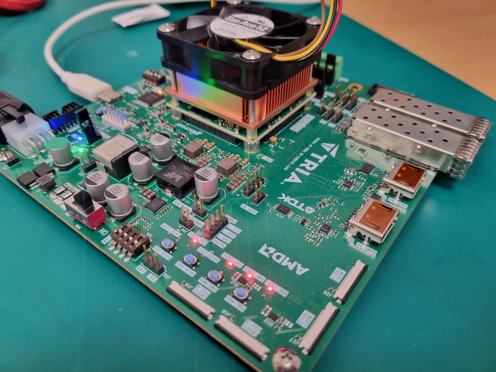
This is one of the boards I have been waiting to get my hands on for a long time: the Tria VE2302 development kit. This is the development kit for the Tria VE2302 SoM and provides developers with four 22-pin MIPI CSI / DSI connectors, two zSFP connectors, HDMI Tx and Rx, along with Gigabit Ethernet and USB 2.0 ports. There is also a TXR2 interface which is capable of being operated with some SYZYGY / ZMod boards, as we will see in future blogs. The board also provides USB UART, JTAG programming, and a CAN interface.
The development kit provides the SoM with all of the necessary reference clocks, including the 200 MHz system clock, along with the HDMI and HSIO reference clocks.
At the heart of the VE2302 development kit is the VE2302 SoM, which measures just 50 mm by 50 mm. It contains not only the Versal Edge AI device with ARM A72 processors, AI Engine tiles, Network on Chip, and programmable logic, but also 4 GB of LPDDR4, 256 MB of Octal SPI, and 32 GB of eMMC. To ease system integration, there is also a USB 2.0 ULPI PHY and an RGMII Ethernet PHY located on the SoM, along with generation of all the necessary power supplies to support the device. Power rails for the SoM are provided by the carrier card to enable the end application to correctly size the power solution.

On board the SoM, the 33.33 MHz reference clock is provided along with an RTC crystal operating at 32.768 kHz. When combined with the VBATT pin provided via one of the SoM connectors, this enables a battery-backed real-time clock.
The I/O is broken out across three 160-pin micro headers, each of which has a specific focus. The first connector, JX1, provides the USB and PHY signals, along with HDIO, PS and LPD MIO, Sysmon, configuration, and clocking connections.
The second connector, JX2, is dedicated to the XPIO from two banks (703 and 702), while the third and final connector, JX3, is dedicated to the GTYP and GTYP reference clocks.
One of the interesting points of the Avnet SoM is how the LPDDR4 pinning is implemented. The LPDDR4 is connected as triplets in XPIO banks 700, 701, and 702, operating at 1.1 V. All but four of the signals are implemented in banks 700 and 701, which means four signals in bank 702 could limit operation to 1.1 V interfaces. This is not suitable for many applications and makes the remainder of bank 702 potentially inefficient, as it cannot be used.
The VE2302 SoM, however, makes use of Answer Record 35358, which enables users to implement an I/O-bank-efficient solution by allowing the developer to set the I/O standard used on bank 702. The developer is then responsible for ensuring proper termination of the signal in the hardware design.
Let’s take a look at building a simple application on this SoM. We can access the board definition files from the Avnet / Tria board definition repository. Once these are visible to Vivado, we are able to create a new project targeting the SoM. These board definition files are important as they define the configuration for the Control Interface and Processing System (CIPS) and the NoC for the DDRMC within Versal.


Once this has been completed, we can quickly and easily export the application to Vitis, create a platform, and run a simple Hello World application on the board. This provides a nice and simple pipe-cleaning exercise to ensure we have everything we need to start development.


This is important, as I am currently developing three courses for the VE2302 SoM and development kit based around the hardware, software, and embedded Linux elements, as I did for the Ultra96, MiniZed, and ZUBoard. Now that I have the board, I can make a start on completing the labs.
FPGA Conference
FPGA Horizons US East - April 28th, 29th 2026 - THE FPGA Conference, find out more and get Tickets here.
FPGA Journal
Read about cutting edge FPGA developments, in the FPGA Horizons Journal or contribute an article.
Workshops and Webinars:
If you enjoyed the blog why not take a look at the free webinars, workshops and training courses we have created over the years. Highlights include:
Upcoming Webinars Timing, RTL Creation, FPGA Math and Mixed Signal
Professional PYNQ Learn how to use PYNQ in your developments
Introduction to Vivado learn how to use AMD Vivado
Ultra96, MiniZed & ZU1 three day course looking at HW, SW and PetaLinux
Arty Z7-20 Class looking at HW, SW and PetaLinux
Mastering MicroBlaze learn how to create MicroBlaze solutions
HLS Hero Workshop learn how to create High Level Synthesis based solutions
Perfecting Petalinux learn how to create and work with PetaLinux OS
Boards
Get an Adiuvo development board:
Adiuvo Embedded System Development board - Embedded System Development Board
Adiuvo Embedded System Tile - Low Risk way to add a FPGA to your design.
SpaceWire CODEC - SpaceWire CODEC, digital download, AXIS Interfaces
SpaceWire RMAP Initiator - SpaceWire RMAP Initiator, digital download, AXIS & AXI4 Interfaces
SpaceWire RMAP Target - SpaceWire Target, digital download, AXI4 and AXIS Interfaces
Embedded System Book
Do you want to know more about designing embedded systems from scratch? Check out our book on creating embedded systems. This book will walk you through all the stages of requirements, architecture, component selection, schematics, layout, and FPGA / software design. We designed and manufactured the board at the heart of the book! The schematics and layout are available in Altium here. Learn more about the board (see previous blogs on Bring up, DDR validation, USB, Sensors) and view the schematics here.
Sponsored by AMD


