MicroZed Chronicles: MathWorks Deep Learning Processor
- Adam Taylor

- Aug 13, 2025
- 4 min read
Updated: Aug 16, 2025
One of the things we have been working on recently is a project that examines telemetry on a satellite. This system uses machine learning algorithms to detect and classify anomalies within the telemetry stream.
My initial solution to this, which will be presented at the FPGA Horizons Conference, was to use TinyML for Microcontrollers coupled with a RISC-V softcore.
This approach worked well; however, for space applications, a software-free solution is often preferred for reasons of reliability and determinism.
Moving Towards a Hardware-Only Solution
As such, towards the end of the project, as we were already heavy users of MATLAB and Simulink for FPGA design, I decided to invest in the Deep Learning HDL Toolbox. The Deep Learning Toolbox allows me to instantiate the MathWorks deep learning processor within any AMD device, from SoCs to traditional FPGAs.
However, after wrapping that project up at the beginning of the year, I have been a little busy and unable to look at the Deep Learning HDL Toolbox until recently.
Inside the Deep Learning HDL Toolbox
At the heart of the toolbox is the Deep Learning Processor (DLP) IP Core, which can be customised to support specific networks before deployment on an FPGA.
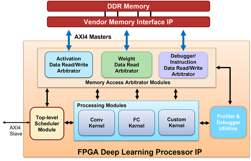
The core connects to the rest of the design via AXI and AXI Lite interfaces:
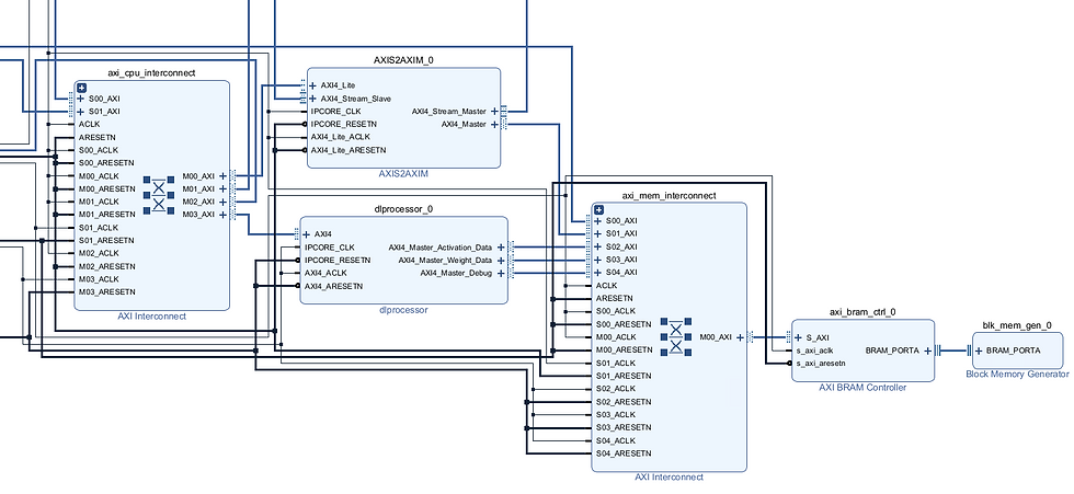
AXI Interfaces – Connect to BRAM or external memory (DDR4/DDR5), where activations, weights, and input data are stored. This could be image data for CNNs or time-series data for LSTM networks.
AXI Lite Interface – Used for control, configuration, and status reporting. This enables control of inference via a finite-state machine if required.
Internally, the DLP IP consists of three processing modules, all customisable in MATLAB:
Fully Connected Kernel – Implements layers with fully connected outputs.
Custom Kernel – Supports custom layers and functions (e.g., sigmoid).
Convolution Kernel – Implements convolution layers.
Getting Started with the Reference Design
The quickest way to begin is by generating a reference design in MATLAB, which in turn generates a Vivado project targeting the ZCU102 evaluation board. The design can be tested directly from MATLAB using a JTAG interface.
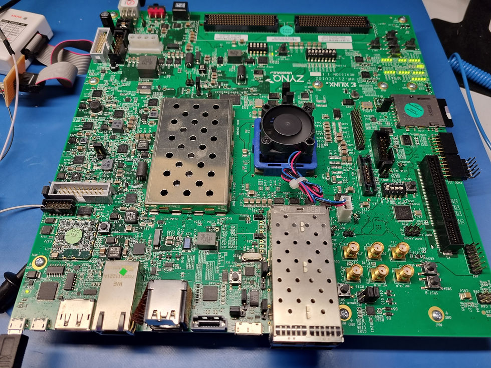
As I already have a ZCU102, I explored this reference design. Once up and running, I can adapt it for new models and test them in hardware recreating the satellite telemetry anomaly detection network.
For my satellite telemetry application, using internal BRAM for weights, activations, and input data is ideal, as it avoids the added complexity and cost of external memory.
Design Architecture Overview
The architecture is straightforward it takes only a few minutes to get an application running.
Although the reference design uses an SoC device, the processor is responsible solely for clocks and reset signals.
The process begins with defining a configuration file for the DLP and its interfaces.
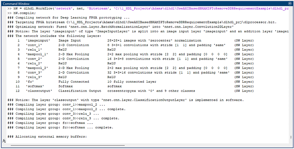
Next, I imported a pretrained MNIST classification network from the MATLAB library. Analysing it reveals the structure of the network to be implemented.
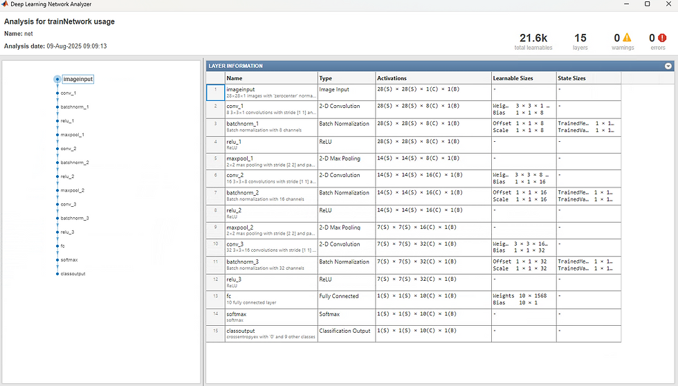
With the network defined, the processor is configured and optimised for it.
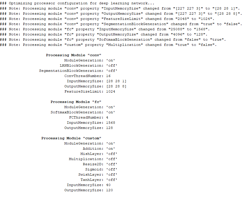


Once the processor has been optimised, we are able to ask MATLAB to build the deep learning processor IP design within Vivado.
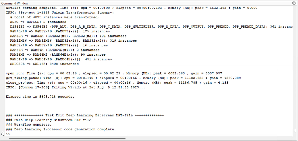
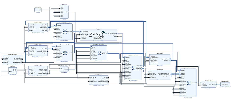
This might take a few minutes, but when it completes you can open Vivado and explore the project. You will see the AXI Interconnects, Deep Learning IP, and the AXI infrastructure.

Building and Running the Design
Once optimised, MATLAB can build the DLP IP design for Vivado. Compilation takes a few minutes, after which the Vivado project reveals the AXI interconnects, Deep Learning IP, and associated infrastructure.
Before running the hardware example, the Zynq Processing System (PS) must be configured correctly no clocks are provided otherwise. This is done by installing the Deep Learning HDL Toolbox Support Package for Xilinx FPGA and SoC Devices from the Add-On Manager.

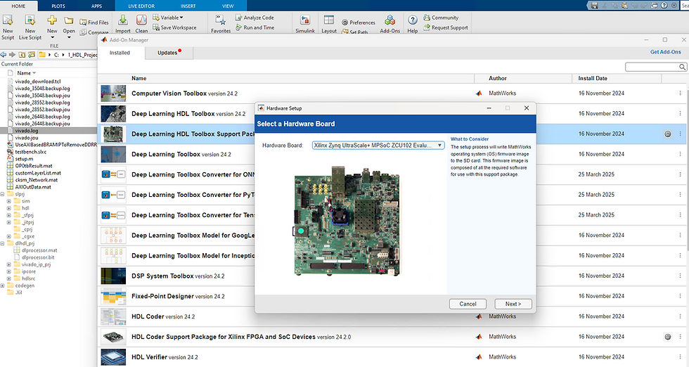
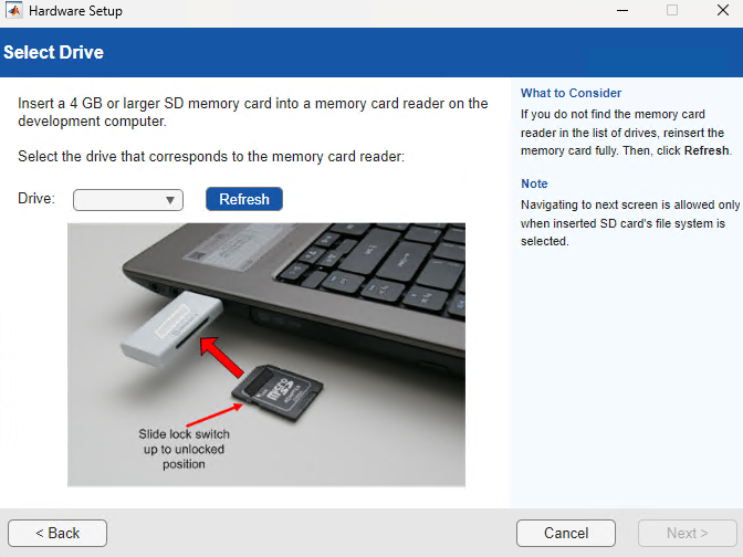
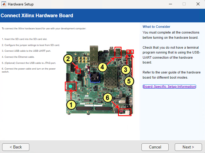
The Add-On Manager also provides tools to program an SD card for the ZCU102, ensuring the PS delivers the required clocks and reset signals.
With setup complete, I powered on the ZCU102, connected JTAG to the development machine, and downloaded the bitstream from MATLAB. This also configures FPGA memories with the network’s weights and activations.

Testing the Network
I then loaded a simple image and performed inference. The MNIST network, trained to recognise handwritten digits, returned a correct prediction via the JTAG link.
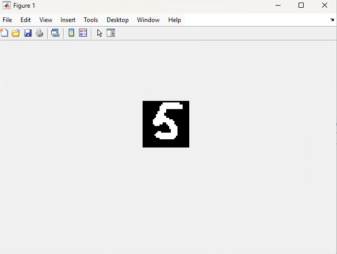

Since profiling was enabled, I could view both the inference result and the performance metrics. While this was a simple network, the speed was impressive.
Next Steps
This exercise has “pipeline-cleaned” the workflow from network definition in MATLAB to deployment and testing on hardware. With the process established, I can now explore transfer learning for more complex machine learning applications, applying the same methodology.
UK FPGA Conference
FPGA Horizons - October 7th 2025 - THE FPGA Conference, find out more here.
Workshops and Webinars:
If you enjoyed the blog why not take a look at the free webinars, workshops and training courses we have created over the years. Highlights include:
Upcoming Webinars Timing, RTL Creation, FPGA Math and Mixed Signal
Professional PYNQ Learn how to use PYNQ in your developments
Introduction to Vivado learn how to use AMD Vivado
Ultra96, MiniZed & ZU1 three day course looking at HW, SW and PetaLinux
Arty Z7-20 Class looking at HW, SW and PetaLinux
Mastering MicroBlaze learn how to create MicroBlaze solutions
HLS Hero Workshop learn how to create High Level Synthesis based solutions
Perfecting Petalinux learn how to create and work with PetaLinux OS
Boards
Get an Adiuvo development board:
Adiuvo Embedded System Development board - Embedded System Development Board
Adiuvo Embedded System Tile - Low Risk way to add a FPGA to your design.
SpaceWire CODEC - SpaceWire CODEC, digital download, AXIS Interfaces
SpaceWire RMAP Initiator - SpaceWire RMAP Initiator, digital download, AXIS & AXI4 Interfaces
SpaceWire RMAP Target - SpaceWire Target, digital download, AXI4 and AXIS Interfaces
Embedded System Book
Do you want to know more about designing embedded systems from scratch? Check out our book on creating embedded systems. This book will walk you through all the stages of requirements, architecture, component selection, schematics, layout, and FPGA / software design. We designed and manufactured the board at the heart of the book! The schematics and layout are available in Altium here. Learn more about the board (see previous blogs on Bring up, DDR validation, USB, Sensors) and view the schematics here.
Sponsored by AMD


