
Renesas ForgeFPGA 2K
- Feb 5
- 5 min read
Programmable logic is very powerful in our solutions. We can perform complex image and signal processing and even accelerate machine learning by leveraging it.
Of course, programmable logic started out as simple glue logic, providing basic processing or interface expansion, and there is still often a need for these capabilities in many applications.
A while ago, we looked at the Renesas ForgeFPGA, which provided designers with 1K lookup tables, on-board oscillator, and the ability to configure from either built in OTP memory or external SPI flash in either master or slave mode.
Recently, Renesas released an updated ForgeFPGA with an increased capacity of 2K LUTs. This time, the device, the SLG47921, also includes 64 KB of BRAM, 10 KB of distributed RAM, true LVDS support for three differential pairs, two I/O banks, a low-frequency 3 MHz mode provided by the internal oscillator, and a second PLL. It is also possible to level shift a signal from one VDDIO domain without the need to pass through the logic fabric.

In discussions with Renesas, I understand that the LVDS pairs have primarily been provided to enable users to drive LCD displays. To support this use case, the LVDS pairs are capable of operation at up to 100 Mbps and can be driven using double data rate.
One nice capability, is the ability to load a different bitstream from the external configuration memory. Up to 16 different bitstreams can be supported via GPIO Controls or directly from the FPGA Core. What makes this particularly interesting is that it is possible to freeze the contents of the BRAM during this update. This means a more complex operation can be configuration-multiplexed, with data values stored in BRAM between bitstreams, allowing solutions to be implemented that would otherwise require more logic resources than are available.
To develop for ForgeFPGA devices, Renesas provides a development board that comes in two parts. The first element, the Go Configure Board, provides a base platform that can be used to program ForgeFPGAs once they are plugged in using a suitable socket card. Each socket card supports a specific ForgeFPGA device. This approach allows developers to use multiple socket boards to support not only different ForgeFPGA devices, but also the wider GreenPAK family. The Go Configure Board also includes programming and power support, along with the ability to generate analogue and digital signals.
Let us take a look at a simple application for which we can use the ForgeFPGA. We will connect an ADC and a DAC, linking the two internally using AXI Stream. This demonstrates the use of I²C and SPI communications when Pmod ADCs and DACs are used, and it also allows us to add filtering within the device at a later point if required.
To get started, we create the RTL source code, currently only Verilog-2005 is fully supported, with partial system Verilog support and a testbench to ensure the design functions as expected.

The next step is to create the project in Go Configure and target the SLG47921V FPGA. Once synthesised, we need to map the I/O of the module to the FPGA pins. The development board is helpfully labelled on the silkscreen, which makes this process straightforward.
For clocking, we use the internal oscillator in its 50 MHz mode. To do this, we need signals in our RTL that can be connected to the oscillator and post-oscillator divider in the FPGA. These connections are made using the I/O Planner. We also need to configure the clock mux to ensure it selects the post-divider oscillator output.


In this view, I also set VDDIO to 3.3 V to ensure compatibility with the Pmod modules.

Once this is completed, we can generate the bitstream and test the design using an Analogue Discovery 3, which provides the input signal and captures the output on the oscilloscope.
The PmodAD2 modules was designed to interface with the I2C ADC on the Pmod and output a AXI Stream. While the PmodDA4 design was developed to receive data from a AXI Stream and output it using SPI to the DAC on the PmodDA4.
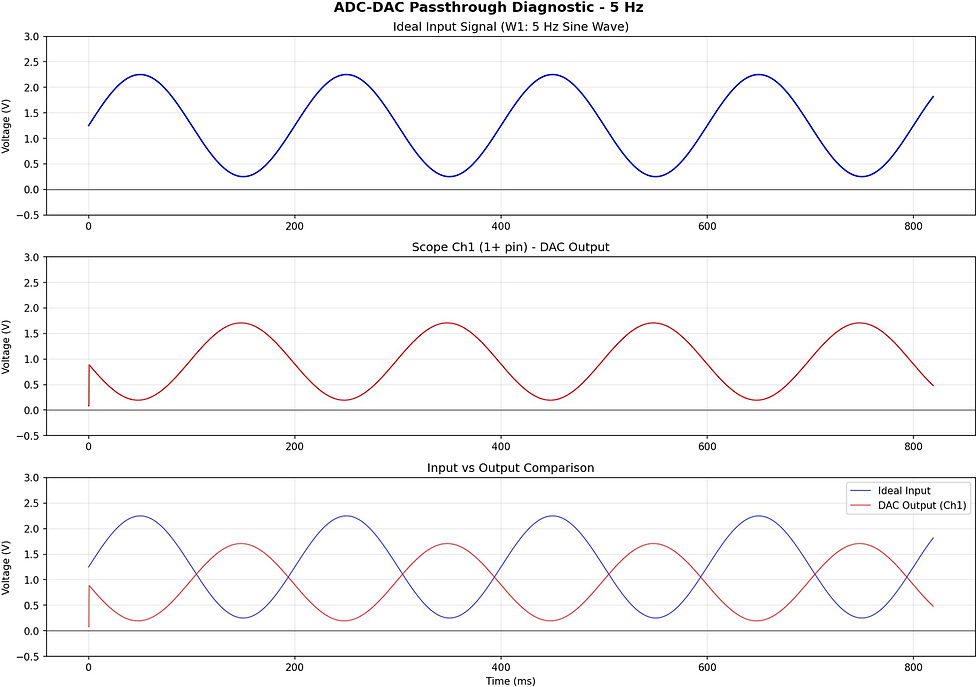
The design works and passes the signal as would be expected the phase shift is of course due to the propagation through the FPGA. While the difference in amplitude is due to the different scaling of the ADC and DAC, and the fact there is no calibration performed on this simple example. We could of course implement calibration within the FPGA and correct for the phase difference if necessary.
All told, these FPGAs are very interesting for applications where a very low-cost FPGA is required. The toolchain is a little different from what you might be used to, but it works well, and once you get to grips with it, it allows you to create effective FPGA-based solutions.
FPGA Conference
FPGA Horizons US East - April 28th, 29th 2026 - THE FPGA Conference, find out more and get Tickets here.
FPGA Journal
Read about cutting edge FPGA developments, in the FPGA Horizons Journal or contribute an article.
Workshops and Webinars:
If you enjoyed the blog why not take a look at the free webinars, workshops and training courses we have created over the years. Highlights include:
Upcoming Webinars Timing, RTL Creation, FPGA Math and Mixed Signal
Professional PYNQ Learn how to use PYNQ in your developments
Introduction to Vivado learn how to use AMD Vivado
Ultra96, MiniZed & ZU1 three day course looking at HW, SW and PetaLinux
Arty Z7-20 Class looking at HW, SW and PetaLinux
Mastering MicroBlaze learn how to create MicroBlaze solutions
HLS Hero Workshop learn how to create High Level Synthesis based solutions
Perfecting Petalinux learn how to create and work with PetaLinux OS
Boards
Get an Adiuvo development board:
Adiuvo Embedded System Development board - Embedded System Development Board
Adiuvo Embedded System Tile - Low Risk way to add a FPGA to your design.
SpaceWire CODEC - SpaceWire CODEC, digital download, AXIS Interfaces
SpaceWire RMAP Initiator - SpaceWire RMAP Initiator, digital download, AXIS & AXI4 Interfaces
SpaceWire RMAP Target - SpaceWire Target, digital download, AXI4 and AXIS Interfaces
Embedded System Book
Do you want to know more about designing embedded systems from scratch? Check out our book on creating embedded systems. This book will walk you through all the stages of requirements, architecture, component selection, schematics, layout, and FPGA / software design. We designed and manufactured the board at the heart of the book! The schematics and layout are available in Altium here. Learn more about the board (see previous blogs on Bring up, DDR validation, USB, Sensors) and view the schematics here.
