
MicroZed Chronicles: EML in FPGA
- Apr 22
- 5 min read
FPGA Conferences
FPGA Horizons London- October 6th and 7th 2026 - get Tickets here.
Recently, a paper was released on arXiv titled “All Elementary Functions from a Single Operator” by Andrzej Odrzywołek from the Institute of Theoretical Physics in Krakow, Poland.
This paper is very interesting. It defines a single operation, eml(x, y), which, when combined with the constant 1, can be used to compute all elementary functions such as exp, ln, sin, cos, addition, subtraction, multiplication, and more.
Across social media and within the paper itself, this eml(x, y) operator has been described as being analogous to a universal gate like NAND. As FPGA implementation was mentioned as one possible realisation, I was tagged quite often as the paper circulated.
The concept is certainly intriguing, and the paper does demonstrate that the eml(x, y) approach can be used to construct any elementary function. However, when it comes to implementation in an FPGA, this approach comes with some important limitations.
At its core:
eml(x, y) = exp(x) - ln(y)
The power of this approach comes from composition. Since exponentials and logarithms can be combined to form multiplication, division, powers, and ultimately trigonometric functions, building trees of the eml(x, y) operator allows the construction of any elementary function.
For example:
exp(x) can be computed in one layer
sqrt(x) in four layers
sin(x) in seven layers
Though, for some functions like sin(x), we also need to support complex numbers.
This is where things get interesting from an FPGA engineer’s perspective.
While eml(x, y) may be mathematically universal, mathematical universality does not imply hardware efficiency. Each eml(x, y) operation requires computing both exp(x) and ln(y). These are not trivial operations in hardware. Common FPGA implementation approaches include:
CORDIC operating in hyperbolic mode
Lookup tables with interpolation
Polynomial approximations
All of these approaches:
Consume DSPs, BRAMs, and registers
Require multiple clock cycles
Introduce latency
Critically, each node in the EML tree is itself a multi-cycle, resource-intensive operation. When composed into a tree, both latency and resource usage grow quickly. This makes the approach significantly less efficient than directly implementing the required function.
This is especially true when developers can leverage:
Vendor IP cores
MATLAB or Simulink
High-Level Synthesis libraries
These tools typically provide highly optimised implementations of elementary functions in terms of both performance and resource utilisation.
In engineering, we should never say never. While the EML approach is not something we would use for most FPGA designs, it does have a niche.
It becomes interesting in resource-constrained designs where:
Flexibility is more important than throughput
A wide range of functions is required
Hardware resources are limited
Rather than building a full EML tree in hardware, a more practical approach is to reuse a single EML unit and sequence operations over time. What this creates is effectively a microcoded mathematical processor where flexibility is achieved through instruction sequencing rather than parallel hardware.
The architecture consists of:
EML unit, which performs exp(x) - ln(y)
Stack for intermediate values
Program ROM which holds instruction sequences for each function
FSM which controls execution
The idea is to implement a simple instruction set, for example:
push_1 to push constant 1 onto the stack
push_x to push input x
push_y to push input y
execute to perform eml(x, y) using stack values
halt to stop execution
Each elementary function is represented as a program stored at a specific offset in ROM. The FSM:
Fetches instructions using a program counter
Manipulates the stack
Triggers the EML unit
Loops until the program completes
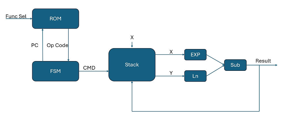
The stack itself does not need to be large. Typically 16 to 32 entries is sufficient. It must support pushing both inputs required by the EML operation.
While this could be implemented directly in RTL, High-Level Synthesis is a very good fit for this architecture. HLS allows:
Rapid architectural exploration
Easier implementation of control logic
Direct use of optimised math libraries for exp and ln
This avoids having to manually implement these complex functions while still enabling hardware realisation.
In this example, a fixed-point implementation was used to reduce resource utilisation. The Program ROM was configured to implement:
exp(x)
ln(x)
A self-checking testbench was used to sweep a range of values and verify correctness.
Results:
C simulation passed within acceptable accuracy
Co-simulation matched C simulation results
Hardware implementation was compact and fitted within a small Spartan-7 device

However, the trade-off is performance:
Each computation requires multiple instruction cycles
Overall latency is relatively high compared to dedicated implementations

The eml(x, y) approach is a fascinating concept and a great example of mathematical elegance.
However, from an FPGA perspective:
It is not the most efficient solution for implementing elementary functions
It introduces significant latency and resource overhead when used directly
That said, when restructured into a microcoded architecture, it becomes a useful tool in specific scenarios where:
Flexibility is required
Resources are constrained
Throughput is not critical
Not a go-to approach, but definitely one worth keeping in the FPGA engineer’s toolbox for the right application.
You can find the example in the Git Repo here.
FPGA Conference
FPGA Horizons London- October 6th and 7th 2026 - get Tickets here.
FPGA Journal
Read about cutting edge FPGA developments, in the FPGA Horizons Journal or contribute an article.
Workshops and Webinars:
If you enjoyed the blog why not take a look at the free webinars, workshops and training courses we have created over the years. Highlights include:
Upcoming Webinars Timing, RTL Creation, FPGA Math and Mixed Signal
Professional PYNQ Learn how to use PYNQ in your developments
Introduction to Vivado learn how to use AMD Vivado
Ultra96, MiniZed & ZU1 three day course looking at HW, SW and PetaLinux
Arty Z7-20 Class looking at HW, SW and PetaLinux
Mastering MicroBlaze learn how to create MicroBlaze solutions
HLS Hero Workshop learn how to create High Level Synthesis based solutions
Perfecting Petalinux learn how to create and work with PetaLinux OS
Boards
Get an Adiuvo development board:
Adiuvo Embedded System Development board - Embedded System Development Board
Adiuvo Embedded System Tile - Low Risk way to add a FPGA to your design.
SpaceWire CODEC - SpaceWire CODEC, digital download, AXIS Interfaces
SpaceWire RMAP Initiator - SpaceWire RMAP Initiator, digital download, AXIS & AXI4 Interfaces
SpaceWire RMAP Target - SpaceWire Target, digital download, AXI4 and AXIS Interfaces
Embedded System Book
Do you want to know more about designing embedded systems from scratch? Check out our book on creating embedded systems. This book will walk you through all the stages of requirements, architecture, component selection, schematics, layout, and FPGA / software design. We designed and manufactured the board at the heart of the book! The schematics and layout are available in Altium here. Learn more about the board (see previous blogs on Bring up, DDR validation, USB, Sensors) and view the schematics here.
All words in this blog were written by a human.


