
MicroZed Chronicles: Bringing Up the Explorer Board
- 2 hours ago
- 4 min read
FPGA Horizons London- October 6th and 7th 2026 - get Tickets here.
The $99 Artix UltraScale+ Explorer Board - learn more here
You cannot have missed my excitement over the past few months about the Explorer Board, which was announced at FPGA Horizons US in April.
After weeks of schematic capture, PCB layout, signal and power integrity analysis, and finally manufacturing, the first ten prototype Explorer boards arrived in my lab on Friday, June 5th.

The timing could not have been better. I had a series of meetings with AMD in San Jose this week and was keen to bring along a working Explorer board to demonstrate. Of course, that meant I only had a few hours available to get the FPGA powered up and running before heading to the airport.
Powering the Explorer
The power architecture of the Explorer board is relatively complex, as the Artix UltraScale+ device requires several supply rails:
Core: 0.85 V
VAUX: 1.8 V
VCCO for High-Performance Banks: Adjustable from 1.0 V to 1.8 V
VCCO for High-Density Banks: 3.3 V
MGTAVCC: 0.9 V
MGTAVTT: 1.2 V
MGTAVAUX: 1.8 V
Typically, the core, VCCO, and VAUX rails are generated using switching regulators, while the MGT supplies are provided using lower-noise linear regulators to ensure optimal transceiver performance.
To support these requirements, the Explorer board uses a Microchip MCP16701 PMIC, which provides eight buck converters and five LDOs. Multiple buck converters can be combined to deliver higher output currents when required. In addition to its flexible power architecture, the PMIC can be configured and monitored over I²C.

On the Explorer board, the PMIC is connected to an RP2040 microcontroller, which manages the power-up sequence and configuration. This combination provides a highly flexible solution and forms the basis for supporting a SZGY-compliant interface.
First Power-Up
Bringing the board up on the bench proved interesting. Before we could generate the required power rails, we first needed to develop firmware for the RP2040 to configure the PMIC's internal non-volatile memory with the correct settings for the application.
Once that was complete, we enabled the outputs and watched the design spring into life.
One of the advantages of using a PMIC is that output voltages can be configured before enabling the rails, allowing us to verify the settings and minimise risk during first power-up.
As an additional precaution, the board design includes zero-ohm links between the regulator outputs and the downstream circuitry. This allowed us to isolate the FPGA and supporting devices during initial testing while we verified the PMIC configuration and output voltages.
Success Over JTAG
The Explorer board is designed to be powered and configured via USB-C. The USB architecture incorporates both the FT2232 and RP2040, providing multiple endpoints for programming and system management.

However, for initial bring-up, dedicated JTAG headers were included to simplify debugging and eliminate any uncertainty in the USB configuration path.
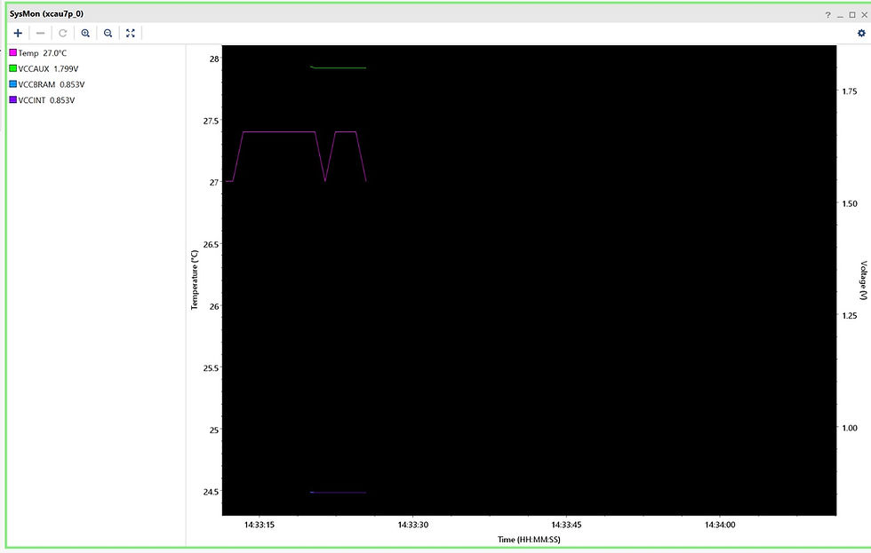
With the zero-ohm links fitted and the PMIC enabled, we were able to verify all voltage rails and successfully detect the FPGA over JTAG. Seeing the device appear in Vivado for the first time is always one of those satisfying milestones that makes all the effort worthwhile.
What's Next?
With the FPGA now powered and accessible, we can begin executing the full board validation plan. This includes:
Signal integrity verification on the high-speed interfaces
Crosstalk analysis
Pmod testing
LED and switch verification
Configuration memory validation
USB and communications testing
This is only the start of the journey, but it is a significant milestone and demonstrates that the core architecture of the board is functioning as intended.
Looking Towards Production
The Explorer board will be the largest production run we have ever undertaken, with approximately 3,000 units planned. As a result, we will be performing extensive thermal and reliability testing over the coming months to ensure the design is robust and manufacturable at scale.
We are also planning another round of pre-production boards and will be looking for beta testers to help evaluate the platform across a range of applications and environments. Join the mailing list to find keep up to date with this,
If you are interested in participating in the beta programme, please get in touch.
It's been an exciting few days, and I'm looking forward to sharing more updates as we continue bringing the Explorer board through validation and into production.
FPGA Conference
FPGA Horizons London- October 6th and 7th 2026 - get Tickets here.
FPGA Journal
Read about cutting edge FPGA developments, in the FPGA Horizons Journal or contribute an article.
Workshops and Webinars:
If you enjoyed the blog why not take a look at the free webinars, workshops and training courses we have created over the years. Highlights include:
Upcoming Webinars Timing, RTL Creation, FPGA Math and Mixed Signal
Professional PYNQ Learn how to use PYNQ in your developments
Introduction to Vivado learn how to use AMD Vivado
Ultra96, MiniZed & ZU1 three day course looking at HW, SW and PetaLinux
Arty Z7-20 Class looking at HW, SW and PetaLinux
Mastering MicroBlaze learn how to create MicroBlaze solutions
HLS Hero Workshop learn how to create High Level Synthesis based solutions
Perfecting Petalinux learn how to create and work with PetaLinux OS
Boards
Get an Adiuvo development board:
Adiuvo Embedded System Development board - Embedded System Development Board
Adiuvo Embedded System Tile - Low Risk way to add a FPGA to your design.
SpaceWire CODEC - SpaceWire CODEC, digital download, AXIS Interfaces
SpaceWire RMAP Initiator - SpaceWire RMAP Initiator, digital download, AXIS & AXI4 Interfaces
SpaceWire RMAP Target - SpaceWire Target, digital download, AXI4 and AXIS Interfaces
Embedded System Book
Do you want to know more about designing embedded systems from scratch? Check out our book on creating embedded systems. This book will walk you through all the stages of requirements, architecture, component selection, schematics, layout, and FPGA / software design. We designed and manufactured the board at the heart of the book! The schematics and layout are available in Altium here. Learn more about the board (see previous blogs on Bring up, DDR validation, USB, Sensors) and view the schematics here.
All words in this blog were written by a human.


