Curiosity Nano
- Dec 30, 2024
- 4 min read
Updated: Jun 24, 2025
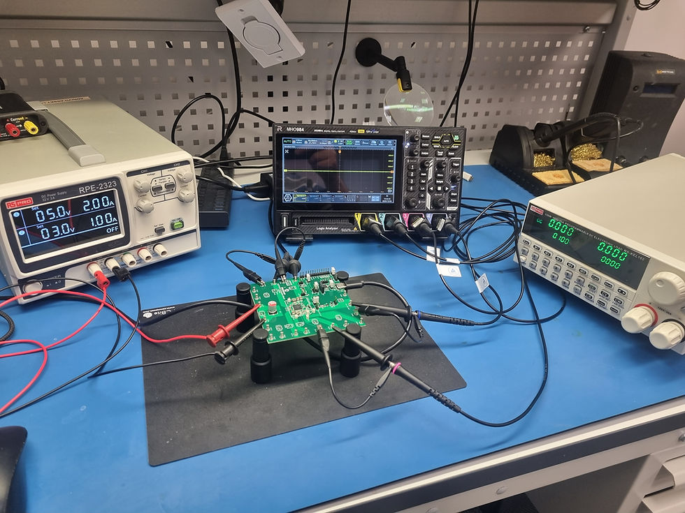
One of the boards purchased in 2024 which was sat in my backlog was the Microchip Curiosity Nano evaluation kit.

This board contains a PIC 16F13145 which along with a 32 MHz PIC16 (8Bit) CPU also provides 14KB of program flash, 1024 Bytes of SRAM, a range of IO interfacing standards, a 10 bit ADC and 8 bit DAC.
However the most interesting aspect of this board is the configurable logic block (CLB) which provides 32 logic look up tables.
Each CLB has 32 basic logic elements, which includes AND/OR/NAND/NOR, D and JK flip flops MUX and 4 input LUT. The CLB inputs can come from either the device IO or peripherals within the processor core such as the PWM. We will examine how we can work with and include the CLB in out design in the next blog. As the first thing we need to do is to create project and run a pipe cleaning hello world project. Once we have this we can add into it the logic design element, I am looking forward to experimenting with the CLB aspect of it as we can create very simple logic design.
To get started with this project we need to download MPLAB X IDE (I used V6.20) and the XC8 8-bit compiler.
Once this is installed we are able to create a new project, the Curiosity Nano development board contains a PIC16F13145 device. Select this device when we use the new project flow.

Select the 8 bit compiler.

Identify a project name and location, click finish.

The next step is to use the MicroChip Code Configurator. The First time you click on this you will see a content download request. Download the required content and we will be ready to begin configuring the system.

This will open the application builder, we can add in the device resources and examples using this to create the application. The initial version will look similar to what is presented below.

From add component select UART Example

This will add the UART Example to the application builder, the key to this is the UART Example tab which shows on the right hand side.

This allows us to configure the example application, and tell us of the steps we need to make to, ensure the application I valid.
Under the configuration instructions, we need to include the UART and ensure it is named UART, configure the IO pins, and enable the UART interrupt.

Using the device resources we can add in the UART, once this has been added we can change the configuration to the correct name and that it is interrupt driven.

We can also change things like the baud rate if desired. We need to ensure the baud error rate is less than 2% for a selected Baud rate.

The final application builder project should look as below.

We also then need to assign the IO pins on the package, the debugger is connected to the PIC using pins TX1 and RX2. These are the pins we need to use to enable the CDC UART in the debugger to work over USB.

Once this is completed we can click on generate, this will generate the source coded and drivers needed to work with the hardware as configured and provide the example application.
Under the example directory, we can see an example application, open the file and copy the code between the dashes (--).

Copy and paste this into the main.c file and build the application.

You will see the total storage required for the program and data space.

Running the application will flash the application to the board and run the example, observing this within a UART terminal will show the hello world message printing out.

Now we have a basic project up and running, we can take a look at getting started with the CLB development and including the logic design in the application.
First I need to solder some headers onto the board.
Workshops and Webinars
If you enjoyed the blog why not take a look at the free webinars, workshops and training courses we have created over the years. Highlights include
Upcoming Webinars Timing, RTL Creation, FPGA Math and Mixed Signal
Professional PYNQ Learn how to use PYNQ in your developments
Introduction to Vivado learn how to use AMD Vivado
Ultra96, MiniZed & ZU1 three day course looking at HW, SW and PetaLinux
Arty Z7-20 Class looking at HW, SW and PetaLinux
Mastering MicroBlaze learn how to create MicroBlaze solutions
HLS Hero Workshop learn how to create High Level Synthesis based solutions
Perfecting Petalinux learn how to create and work with PetaLinux OS
Boards
Get an Adiuvo development board
Adiuvo Spartan 7 / RPi 2040 Embedded System Development Board
Adiuvo Spartan 7 Tile - Low Risk way to add a FPGA to your design.
Embedded System Book
Do you want to know more about designing embedded systems from scratch? Check out our book on creating embedded systems. This book will walk you through all the stages of requirements, architecture, component selection, schematics, layout, and FPGA / software design. We designed and manufactured the board at the heart of the book! The schematics and layout are available in Altium here Learn more about the board (see previous blogs on Bring up, DDR validation, USB, Sensors) and view the schematics here.