
Creating a Nios V/m Hardware Subsystem
- Sep 19, 2022
- 2 min read
In our last blog, we looked at the new Nios V soft-core processor for use in our Intel FPGAs. In this blog, we are going to explore how to create the hardware element of the Nios V design using Quartus Prime and Platform Designer while targeting the Agilex F-Series Transceiver-SoC Development Board.
To get started, we first need is a Nios V license which is available free of charge from the Intel Self-Service Licensing Center. Select the Nios V options and download and install the licenses in Quartus Prime. If you do not have a Quartus Prime license you can also create a 90-day trial license.
With the licenses installed and Quartus Prime open, we are ready to start creating our application. We will do this from a blank project and not use one of the template applications because it is often good to know how to create designs from scratch.
To implement this project, we are going to use the following flow in Quartus Prime and Platform Designer.

The first thing we are going to do is create a new project targeting the Agilex board.


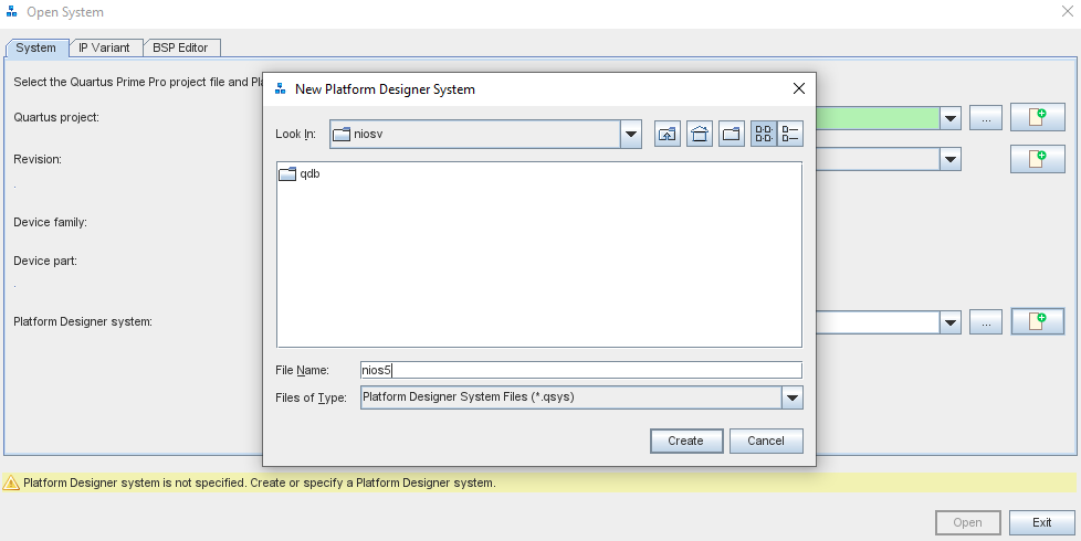
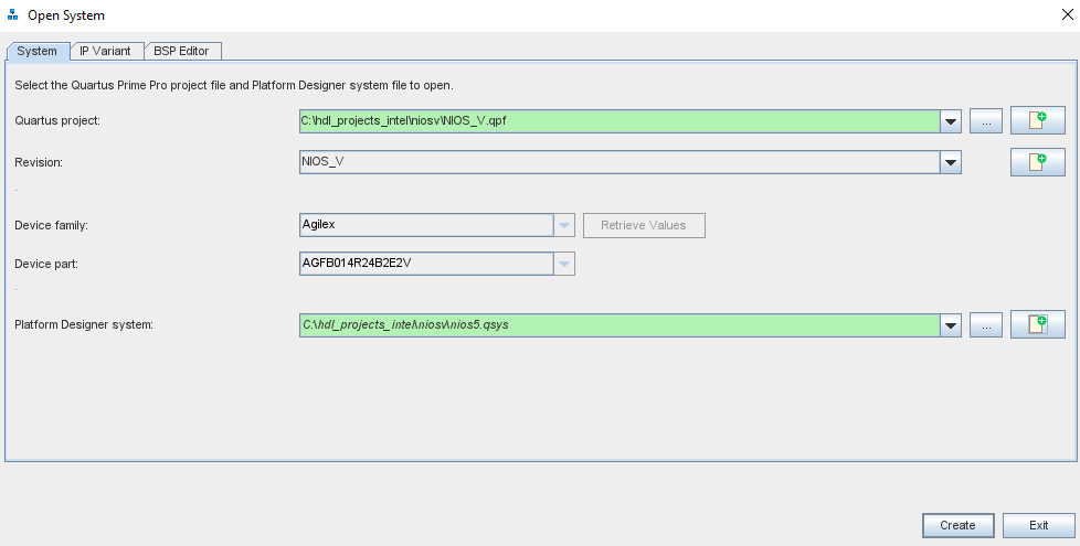
With the project created, the next step is to create a new Platform Designer project. From the menu, select Platform Designer and create a new Platform Designer system at the open dialog. Be sure to name this the same as the top-level entity / module in the project creation.


Creating the Platform Designer system will result in a new Platform Designer project which contains both reset and clock bridges. Ensure the clock bridge is set for the frequency of the input clock which in this case, is 100 MHz. Also make sure that reset is set appropriately for the correct level (e.g., active high or low). For the Agilex F-Series Transceiver-SoC Development Board the reset is active low.

We need to add in the following IP from the IP catalog.
NIOS V/m – Set the vectors reset and exception agents to the on-chip memory
On-Chip Memory 2 – Set the memory size to 131072
JTAG UART
Reset release IP
Connect the clock and reset bridge outputs to all the IP blocks just added and connect the instruction master to the on-chip memory. Connect the data master to the on-chip memory and the JTAG UART. Connect the interrupt from the JTAG UART to the Nios V interrupt port.
Finally connect the reset release IP to gate the reset of the reset bridge output. The final configuration of connections can be seen below.

With the IP configured, the next step is to assign the address of the IP on the instruction and data masters.

The completed system can also be viewed as a schematic.

We can now save the design and generate the HDL files for inclusion in the Quartus Prime project.

Once the files have been generated, we are able to close Platform Designer and implement the project in Quartus Prime. We do need to assign the clock and resetn pins in the IO assignment before we compile the design. Once completed, we will have the SOF file that we can program into the Agilex board to instantiate the Nios V/m processor where we can then run the application software that we will develop in our next blog.


