
Beyond the Fabric: Designing with Agilex 3 FPGAs on Custom Boards
- Jul 28, 2025
- 4 min read
Updated: Aug 29, 2025
When we delve into the world of FPGAs, our minds often gravitate towards the logic design, DSP implementation, and of course meeting timing closure. We often tend to focus on the application such as image processing, robotics and machine learning and the detailed algorithms required. However before we can deploy our application or even test the algorithms performance on a device, there's a crucial foundational step: successfully integrating the FPGA onto a custom board, like the Terasic Atum A3 Nano shown below.

Today, we're taking a different approach. Instead of peering into the Agilex 3 FPGA, we're going to look at what's needed to design it into the board.
After all, the most powerful FPGA is little more than a paperweight if it can't be correctly designed into a functional system. So, let's explore some key concepts essential for a "chip-down" understanding of Agilex 3 board design.
To begin, let's identify the different types of I/O provided on an Agilex 3 device, as understanding these is fundamental to proper board layout and power delivery. These can be broadly grouped as follows:
Clocks and PLLs: These are highly specialized, dedicated I/O pins that form the backbone of the FPGA's timing. They connect directly to the internal clock resources and distribution network, ensuring a stable clock. The clock input can be either single ended or differential, with the ability to terminate on chip (differential, series and parallel) to improve signal integrity. There are also a number of single and differential clock output pins.
Voltage Supplies: As you would expect for a high-performance device, the Agilex 3 requires a diverse array of voltage supplies. From the core voltages that power the logic fabric (either 0.75V for -7S variants or 0.78V for -6S) to various reference voltages (typically 1.2V or 1.8V). A significant benefit is that many reference voltages can, and often should, share the same supply and power plane on your board, simplifying power delivery.
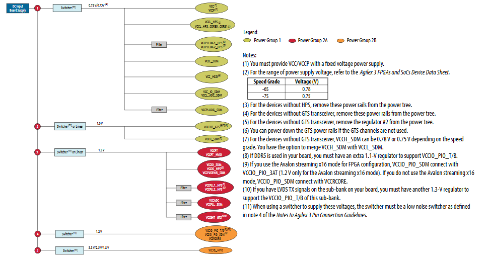
When it comes to I/O, a thoughtful design choice is the splitting of each High-Speed I/O (HSIO) bank into two sub-banks, each capable of operating from different supply voltages. This offers valuable flexibility for interfacing .
When it comes to sequencing the voltage supplies are grouped into three groups (1, 2A and 2B). The sequencing of these groups is one key consideration when designing the board.


High-Speed I/O (HSIO): These banks are provided to enable high-throughput communication. Each HSIO bank consists of 96 I/O pins and features two sub-banks, each with its own VCCIO and 48 I/O pins. Each bank also incorporates two hard memory controllers. These dedicated controllers are optimized for implementing 32-bit LPDDR4 interfaces at speeds up to 2133 Mbps, offering a robust and efficient path to external memory. For scenarios requiring greater customization or alternative memory types, these hard controllers can be bypassed, allowing a soft memory controller to be implemented directly within the FPGA fabric.
High Voltage I/O (HVIO): With 20 I/O pins per bank, the HVIOs are designed to support higher LVTTL and LVCMOS voltage standards. They are also capable of supporting RGMII interfaces at 1.8 Volts, making them ideal for a range of communication protocols that require slightly higher voltage levels than the HSIO.
Configuration Interface: These pins are a mix of dedicated and dual-use, primarily governing how the FPGA is programmed and initializes. Dedicated pins include the essential JTAG interface (for debugging and programming), the oscillator for the Secure Device Manager (SDM), and pins providing configuration status and request signals. We are able to configure the device using JTAG, CvP over PCIe, Avalon ST which uses an external Microprocessor or CPLD and Serial Configuration using QSPI.
Secure Device Manager (SDM): The SDM pins, also split between dedicated and optional, are critical for defining how the SDM operates during configuration and what modes of configuration the device utilizes. The SDM plays a vital role in device security and configuration integrity.
Voltage Sensor Pins: The Agilex 3 incorporates dedicated pins for voltage sensing. These include ADC references and differential input pins for the Analog-to-Digital Converter (ADC) sampling. These are instrumental for monitoring internal voltages and ensuring the device operates within its specified parameters. The voltage sensor provides 7 bit quantisation sampled at up to 1 Kilo Sample Per Second. This allows the device supply voltages to be monitored and verified during operation, something which is critical for high reliability and secure applications.

Hard Processing System Pins: Some Agilex 3 devices include a Hard Processing System, this comes with a range of dedicated pins associated with HPS support. This will include clocks, IO peripherals and of course memories.
Gigabit Transceivers: Multi Gigabit Transceivers, able to get data on and off chip and very high bandwidths. Supporting protocols such as Display Port, 10 / 25G Ethernet and JESD. These pins include not only the TX / RX differential pairs but also termination and supply voltages.
Miscellaneous Pins: This category encompasses a variety of important pins that might not fit neatly into other groups. Examples include pins for setting On-Die Termination (ODT), which is crucial for signal integrity on high-speed interfaces, and pins for remote temperature diode sensing, allowing for accurate remote thermal monitoring.

Understanding these diverse I/O types and their specific requirements is the first fundamental step in designing a custom board for an Agilex 3 FPGA. It's about laying the groundwork, ensuring the FPGA receives the right power, clocks, and connections to truly unleash its potential. In future discussions, we'll dive deeper into specific design considerations for each of these categories, but for now, remember: successful FPGA design starts long before the logic gates are instantiated, it begins with a solid foundation on the board.
Useful links
UK FPGA Conference
FPGA Horizons - October 7th 2025 - THE FPGA Conference, find out more here.
Sponsored by Altera


