
Quartus Prime Lite Flow
- Adam Taylor

- May 16, 2022
- 4 min read
Updated: Jun 26, 2025
So far on our journey exploring Intel devices, we have examined the range of devices and tool chains used for development. In this blog, we are going walk through our first project creation with a simple application. The target board for this will be the DE10-Lite which contains a Intel MAX 10 FPGA. The DE10-Lite is a great board to get started with because it contains a range of memories, sensors, and interfaces that allow us to create interesting projects. It includes 64 MB SDRAM, an accelerometer, Arduino Shield, VGA output, LEDs, switches, and a seven-segment display.

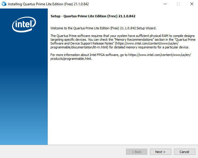
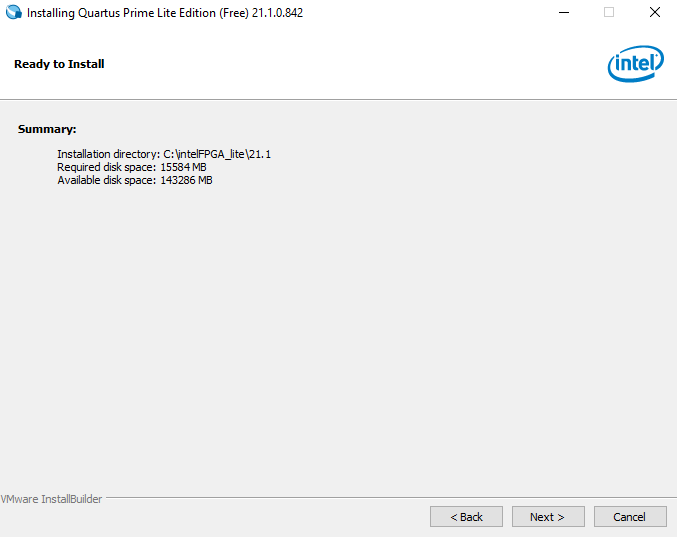
To get started with our application, we first need to install the Quartus Prime software. Since we are working with the MAX 10 devices, we can install the lite version of Quartus Prime which is free from licensing. I downloaded and installed the latest version 21.1 from the Intel website <link>.
Once it was downloaded, I extracted the Tar and installed the Quartus Prime Lite Edition.


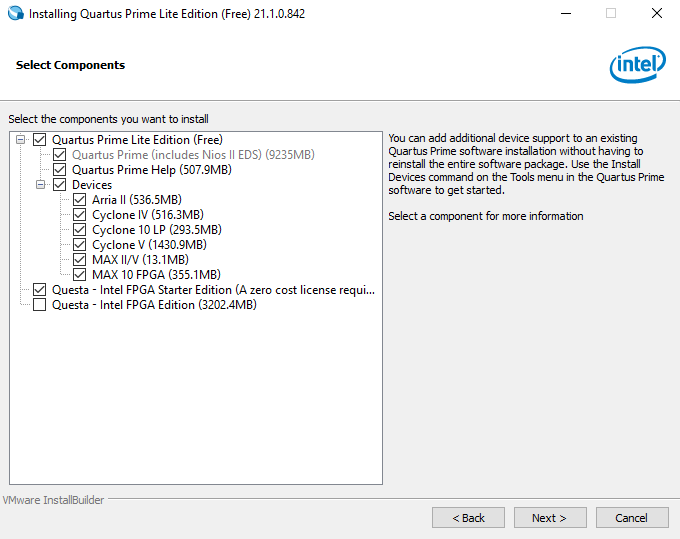


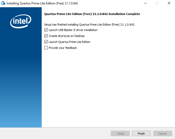
I installed all of the devices, along with Questa-Intel FPGA Starter Edition. Once installation was complete, I selected the run Quartus Prime software.

This will open the Quartus Prime Lite software development environment. Using this environment, we are able to create new projects, compile designs, perform timing analysis, generate bit files, and debug applications in the hardware. As we will see in later blogs, we can leverage IP and create embedded processing solutions utilizing NIOS 2 soft processors and Arm core-based hard processors.

The stages of implementation within Quartus Prime Lite can be seen on the left of the environment, half way down the screen.
Analysis and Synthesis – The first stage of implementation is analysis. Here, the design is analyzed for syntax errors, logical consistency, and boundary connectivity. Once analysis is complete, the design is synthesized into a netlist which implements the registers and look up tables contained within the adaptive logic modules of the FPGA. The synthesis engine will take advantage of any specialist structures in the FPGA logic like memory blocks and DSP blocks.
Fitter – Implements the netlist created by the synthesis stage into the target device. First it fits the ALM, memory blocks, and DSP blocks etc. to locations available within the device. Once the logic elements have been assigned locations by the fitter, the final stage is to route the connections between them. The fitter is guided by timing constraints to help ensure that the desired performance is achieved.
Assembler – Generates the programming file for the FPGA.
Timing Analyzer – Performs static timing analysis enabling the designer to ensure that the implemented design is complaint with the timing performance.
EDA Netlist Writer – Generates the post implementation netlist for back-annotated simulation.
Program Design – Downloads the FPGA or PROM file onto the target board.
To get started with our first project, we are going to create a new Quartus Prime project. We can find this under the main file option menu.

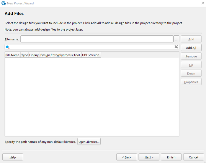
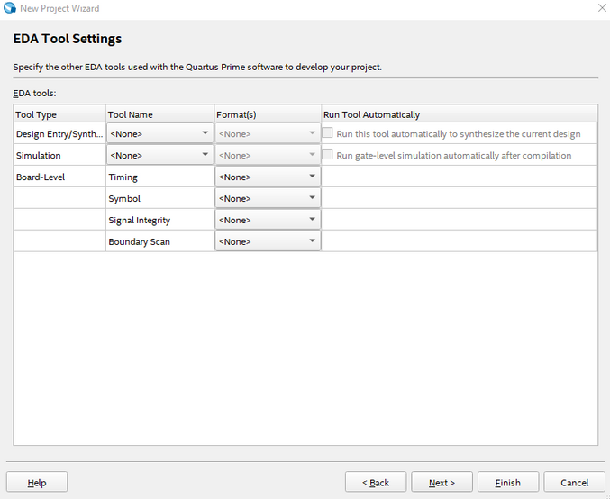
This will open the new project wizard. This wizard will walk us through the creation of the project, any source files, and the target device and board. For this example, I am going to create an empty project called blog3 with the top entity called led_fsm. Initially no files are added and the project is configured to target the MAX 10 DE10-Lite board without a top-level design file.


Once the project has been created, the next step is to create a new VHDL / Verilog file.


For this project, I will be creating a VHDL file. Once the file is created, add in the simple code below which will enable you to control the LEDs via the switches. Note how the entity architecture name is the same as the one I declared as the top entity when I created the project using the project wizard.

Once this is entered, save the file to your desired location. I stored them within the project. Under the project navigator, notice we can change the view to explore hierarchy which is useful when we have large designs, design files, IP components, and design units along with revisions.

Under the tasks section, we are able to change the view between Compilation which shows the basic stages of implementation. Full design shows the entire design flow from project creation to engineering change orders, SSN and power analysis. Gate level simulation aids performance of back annotated simulation. RTL simulation configures the project for initial verification using functional simulation of the RTL. Rapid recompilation enables faster recompilation of the design when design changes are required.

Using the Compilation view, run the analysis and synthesis. Once completed, select pin planner from the menu bar and assign the signals from the design to the IO as below.

Once the pins are assigned, close the pin planner and run the fitter and assembler.

With the compilation completed, we can then connect ourDE10-Lite board over USB to the development machine.
We can now download the FPGA programming file by running the program device. This will open the device programmer in a new window. Ensure that the hardware setup shows the USB-Blaster and mode of JTAG, check the program / configure box and press start.

This will download the programming file to the DE10-Lite board and enable us to change the LEDs using the switches. SW[3] is the enable switch which when high enables the other switch to control the LEDs. You can see when the switch is enabled as the first LED will be illuminated.
Now that we have had a basic walk-through of the tool and the implementation of our first project, we will begin to look more closely at deeper aspects of the tool.


