
Efinix Trion FPGA and Xyloni Development Board
- May 20, 2022
- 4 min read
Updated: Jun 26, 2025
I have heard several attendees mention Efinix FPGAs at a few conferences I have recently attended. As such, I thought I would take a quick look at the devices and architectures and also examine the tool flow in order to create a simple example design.
Let’s start at the beginning. Efinix was founded in 2012 and offers two families of devices: the Trion and Titanium. Both Trion and Titanium devices are based on Quantum architecture which is based on eXchangable Logic Routing (XLR). The later Titanium device range, however, has upgraded XLR compared to what is offered in Trion. An XLR cell can be configured to function as either a logic cell with a LUT, register and adder, or routing matrix. This approach provides a finer grained architecture that offers interesting flexibility and very efficient use of silicon. As FPGA designers, we know that some devices require more logic and others require more routing. An interesting fact about the upgraded XLR in the Titanium family is that it enables more logic than the data sheet states.
Trion FPGAs – Offers densities from 4K to 120K logic elements and are fabricated on the SMIC 40LL process. Along with the Quantum fabric, the device provides PLL, oscillators, and a wide range of interface standards including LVDS, MIPI, and DDR (DDR3, LPDDR3 and LPDDR2).
Titanium FPGAs – Offers densities from 35K to 1M logic elements and are fabricated on a 16 nm node. These devices offer a mix of GPIO, high speed IO, MIPI, Serdes (16 Gbps and 25.8 Gbps) along with DDR (DDR4 and LPDDR4) and PCIe Gen4 support.
What is interesting with respect to Efinix is how the Efinity development environment is provided. There is no free web version which is limited to specific devices. Instead, you must buy a development kit which can be registered and provides access to the software. The cheapest development board available is the Xyloni board which retails for $35.
The Xyloni board provides the developer with a Trion T8 device, 128 Mbit SPI, USB UART, 41 pin connector, 12 pin Pmod, four user LEDs, and two push buttons. The board is very compact and fits within a small tin.

It also comes with the necessary headers and USB cables to get us up and running quickly. The product code needed to register the software can be found on the cardboard case that protects the metal tin.
Once the board is registered and we’ve downloaded the software, we can get started creating our first application. This application is purposely simple and works with the LED and push buttons to enable easy understanding of the tool flow.
With the Efinity software open, the first thing we need to do is to create a new project.

A new project can be created from either the file menu or the new project icon on the menu bar.

This will open the new project wizard. Enter the project name and location of the project along with the family, device, and timing model. In this case, use the T8F81C2.

The next element is to include the RTL file and the simple constraints file. The board provides a 33.33 Mhz oscillator.

The project will open and we can see the dashboard on the top left which will help us do synthesis, place and route, and bit file generation.

The next step is to run the synthesis. Once this is complete, we are able to connect the core logic to the device interfaces.
Once synthesis has completed, you will see that there are five unassigned ports. We need to open interface designer to connect these ports to the device interfaces.

When interface designer opens, we will see the device we’ve selected, the IO banks, GPIO, oscillators, PLLs and JTAG.

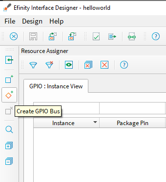
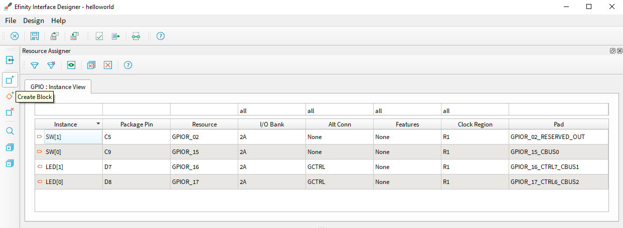
Show the GPIO Resource assigner

Create a GPIO bus one for the LED that is two bits wide and another for the SW input that is also two bits wide.


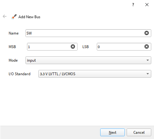


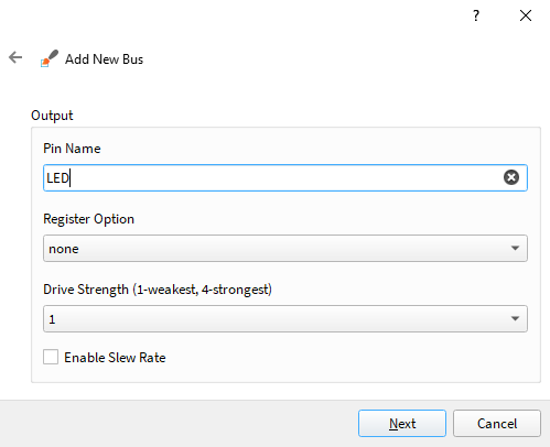
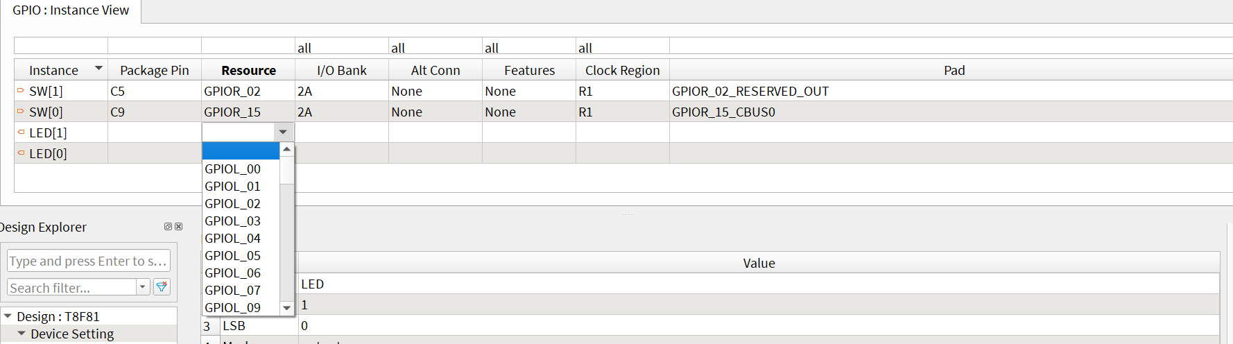
Once the buses have been created, we need to connect up the buses to the GPIO resources. The SW is connected to GPIOR_02 and GPIOR_15 and the LED is connected to GPIOR_16 and GPIOR_17.


The next step is to create a GPIO block. This will be called GPIO_INST5. Change the name to clk (which is the name of the clock) in the block editor. Note: make sure all of the names are in the correct case because it is case sensitive.

Connect the clk port to GPIO_L20 which is on the clkin pin

Once this is completed, we can check the design and export the constraints file.


With the IO constraints defined, the final step is to complete the place and route and generate the bit file. It takes only a few minutes to implement because the design is small.

Once the bit file is available, we are able to download the programming file to the FPGA or the SPI using the Efinity programmer. Note: make sure you have installed the necessary drivers for the Xyloni board as defined in the user manual.
Overall, the development process was smooth and the tool easy to work with. I also purchased a larger T120 Trion development kit that I will create a more serious project on when I get some time!