
Creating a Nios II Processor
- May 30, 2022
- 3 min read
Updated: Jun 26, 2025
FPGAs are great for high performance, low latency, deterministic applications. When it comes to implementation of sequential structures for control and communication, we can implement Finite State Machines (FSMs). For more complex structures though, it is more efficient to use a softcore processor. In the intel family of FPGAs, one of the most popular softcore processors is the Nios II processor which is a 32-bit Reduced Instruction Set Computer (RISC).
As a softcore processor, Nios II can be implemented in any FPGA or SoC within the Intel FPGA range.
In this blog, we are going to look at how to create a Nios II processor targeting the DE10-Lite board using Quartus Prime Lite and platform designer. This will enable us to look at the software environment and run our first application in the following blog.
To get started, first we need to create a new project targeting the DE10-Lite development board


Once the project is open, the next step is to use platform designer to create the Nios II system. Platform designer is Intel’s system integration tool that allows us to work in an IP-centric manner.
We can open platform designer from the tools menu.

Once opened, platform designer will open a blank canvas which includes only a clocking block and reset inputs.

Here we are going to add in the Nios II system and the associated peripherals that are necessary to create a bare minimal system.
The first element to add in is a Nios II processor from the IP library on the left.

Once this is added, we can configure the Nios II as we desire. For this example, we will be using Nios II/e which is the smallest of the available core footprints.

From the IP library, we are also going to add the following:
PIO configured as an output to drive the LEDs on the DE10-Lite board
JTAG UART to enable communication with the host machine
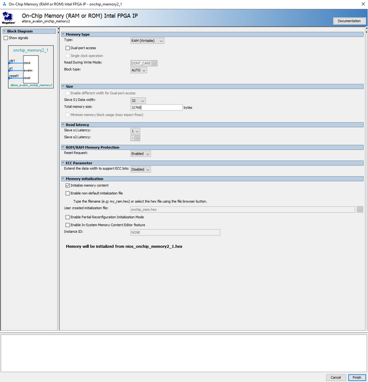
On-chip memory 32K – This is where our program will execute from


Once we have all the peripherals inserted in the system, we need to connect the together in the platform designer. The clock and reset are connected to each peripheral in the system. The data and instruction masters are also connected to the PIO, on-chip memory and JTAG UART.

The clock and reset will be inputs into the FPGA and have already been exported when the project was created. The PIO outputs will also be used to drive the LEDs on the board so we need to export them from platform designer. We can do this by selecting the signal, right clicking, and exporting them.

The final stage of the work in platform designer is to assign the addresses and interrupts.

In the address map, we can see that the on-chip memory starts at address 0x0000_8000. It is from this memory that we will execute the software application. We need to select the Nios II instantiation. On the vectors tab, ensure that the reset vector and interrupt vectors point to the on-chip memory.

With that complete, we can save the design and generate the HDL which will be implemented by Quartus.

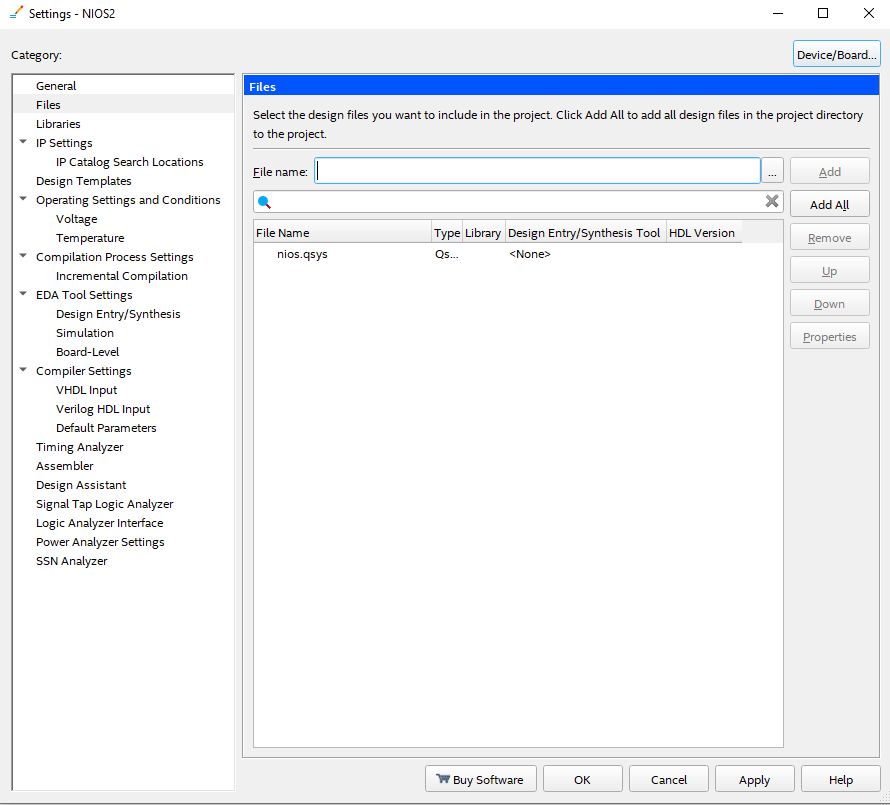
Back in Quartus, we need to add in the platform designer files to the project and set it as the top-level entity.
The final stage prior to implementation is to assign the clock, reset, and LED signals to the IO pins. The clock will be supplied by the 50MHz oscillator (P11) and the reset will be connected to a switch (C10) and the LEDS (A8,A9,A10,B10,D13,C13,D14,A11). Putting the switch to logic 0 puts the design into reset, while logic 1 removes the reset.

Once the pins are allocated, we can compile the design and generate the programming files.

Now we know how to create the softcore processor and peripherals within the FPGA. We will look at how to create the application software in the next blog.


